TM 11-6625-486-14&P
secondary of T501 applies ac voltage to neon lamps I702
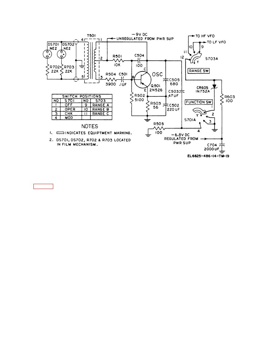
5-7. Modulator and Dial Lamp Power Circuit
and I1703. Current is limited by R702 and R703.
c. The collector of Q501 receives unregulated dc
voltage from the T501 center tap. Forward base bias is
a. The modulator is a transistorized 900-Hz
established through R501 and R502. Emitter bias resistor
oscillator. The modulator amplitude modulates the vfo dc
R503 limits emitter current to a safe value. Capacitor
supply and provides ac power for two neon dial lamps in
C502 bypasses audio frequencies to ground. Harmonic
the filmstrip mechanism. This circuit receives operating
frequencies existing at the collector of Q501 are bypassed
power at all times except when unit power is off.
through capacitor C505. Capacitor C504 connected
Modulation is supplied when FUNCTION SW S701 is set
between the collector and emitter is for stabilization
to MOD and the appropriate vfo is selected by RANGE
purposes. The 900-Hz collector output signal is directed
SW S703.
through coupling capacitor C502 to contact 4 of
FUNCTION SW S701.
The collector of Q501 is
b. The oscillator circuit is the transistorized version
terminated in resistor R505 to provide a constant load
of a Hartley oscillator.
Feedback necessary for
resistance and prevent changes in load current with
oscillation takes place from the collector to the base of
different positions of S701. When switch S701 is in the
Q501 through transformer T501, R504, and C501.
MOD position, modulation is applied to the vfo supply
Frequency of oscillation is determined by C501 and T501.
voltage through Zener diode CR605 and RANGE SW
The center tap on the primary winding of T501 is located
S703. With the FUNCTION SW S701 in any other
to provide an impedance match between the collector and
position, diode CR605 is grounded and causes it to
base circuits. With this arrangement, T501 acts like an
function as a regulator for the variable frequency
auto transformer. Voltage stepup action through the
oscillators.


 Previous Page
