TM 11-6625-486-14&P
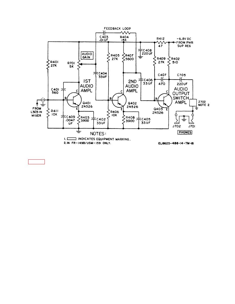
amplified audio signal appears at collector load resistor
5-6. Audio Amplifier Circuit
R407 and is directed through C406 to Q403.
a. The transistorized audio amplifier receives the
c. Transistor Q403 has the emitter grounded and its
mixer signal and amplifies the signal to headphone level.
base receives sufficient forward base bias voltage through
The first two stages of the amplifier follow general circuit
R409 to cause saturation. In this condition, the collector
practice for incorporation of a feedback loop. This loop is
conducts at maximum current through load resistor R402
completed from the collector of Q402 back to the AUDIO
in the absence of an input signal and partially-ceases
GAIN control which is the collector load resistor for Q401.
conduction with a positive going input signal. It operates
The combination of R701, C403, and R404 increases the
like a switch which is normally on. With no input signal
gain of these two stages for the audiofrequencies while
(beat note), only noise will be heard in the headset.
sharply reducing the gain for other frequencies.
When a beat note is present, Q403 will partially cease
conduction and result in a sufficient decrease in noise
level so that only the beat note will be heard. In this
b. The base of transistor Q401 is forward-biased by
respect, the circuit functions as a noise limiter. The
a voltage divider consisting of R401 and R411. Capacitor
transistor stage has negative feedback stabilization from
C401 supplies negative feedback and C409 bypasses
collector to base through capacitor C407. Decoupling
undesirable frequencies. Emitter bias is furnished by
resistor R412 and capacitor C408 keeps audio out of the
R403. Capacitor C402 bypasses audio frequencies. The
power supply. Capacitor C410 couples the collector
applied mixer signal causes variations in the collector
output signal (through filter Z702 (AN/USM-159B only)) to
current of Q401 which is applied through coupling
the PHONES jacks. The PHONES jacks are nonshorting
capacitor C404 to Q402. Forward base bias in this stage
type and, without the headset plugged in, the collector of
is provided by resistors R405 and R406. Emitter bias is
Q403 looks into an open load circuit.
provided by R408 which is bypassed by C405. The


 Previous Page
