TM 11-6625-486-14&P
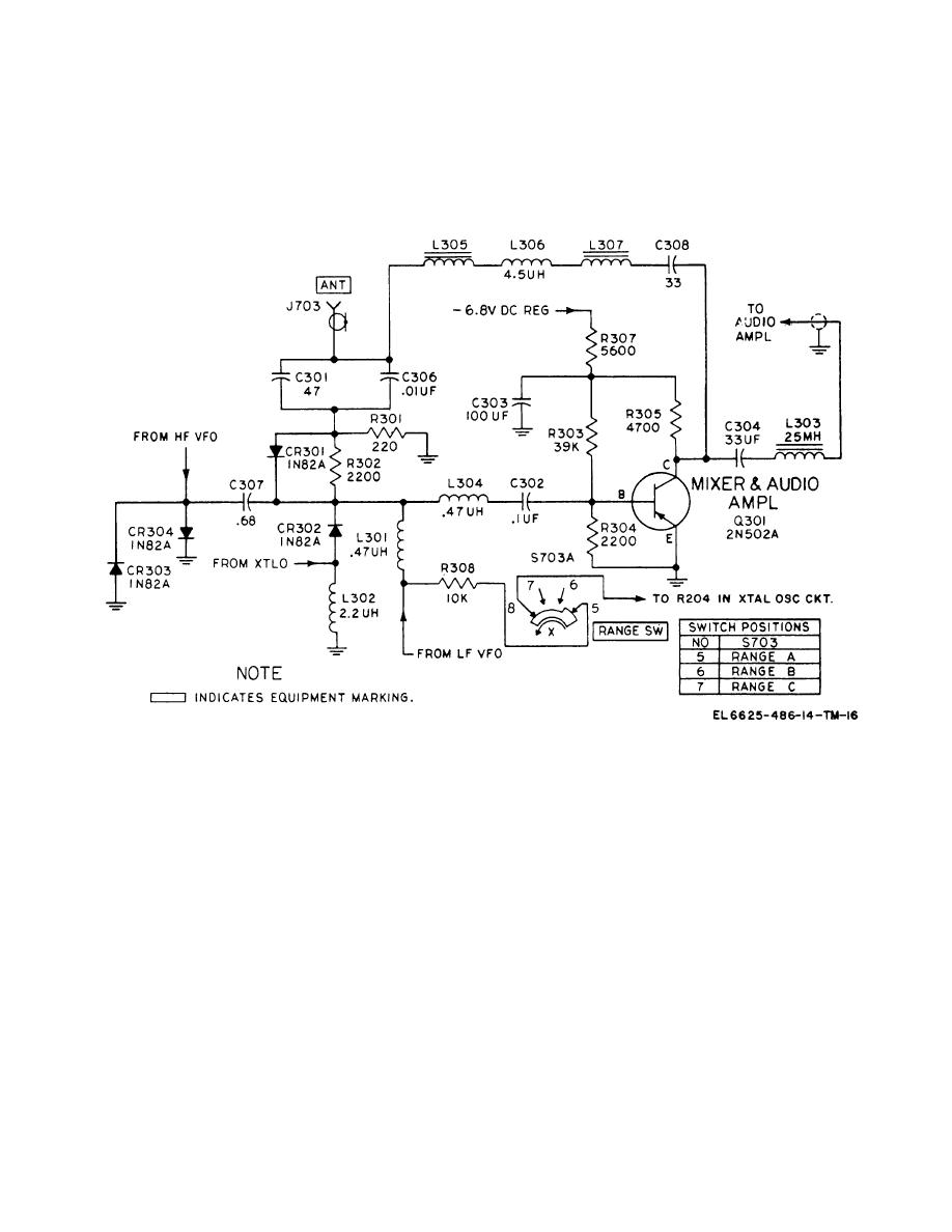
The output signal of Q2 is applied through C12 to a mixer
and C10 at 900 Hz is sufficient to prevent the bypassing
circuit. During modulation, both the oscillator and buffer
of audio frequencies while still providing an effective rf
stages are modulated by pulsing the dc supply voltage at
bypass.
a 900-Hz rate. The reactance of bypass capacitors C8


 Previous Page
